Peter Lobner
Announced on 29 January 2013, DARPA is conducting an intriguing program known as VAPR:
“The Vanishing Programmable Resources (VAPR) program seeks electronic systems capable of physically disappearing in a controlled, triggerable manner. These transient electronics should have performance comparable to commercial-off-the-shelf electronics, but with limited device persistence that can be programmed, adjusted in real-time, triggered, and/or be sensitive to the deployment environment.
VAPR aims to enable transient electronics as a deployable technology. To achieve this goal, researchers are pursuing new concepts and capabilities to enable the materials, components, integration and manufacturing that could together realize this new class of electronics.”
VAPR has been referred to as “Snapchat for hardware”. There’s more information on the VAPR program on the DARPA website at the following link:
http://www.darpa.mil/program/vanishing-programmable-resources
Here are a few of the announced results of the VAPR program.
Disintegrating electronics
In December 2013, DARPA awarded a $2.5 million VAPR contract to the Honeywell Aerospace Microelectronics & Precision Sensors segment in Plymouth, MN for transient electronics.
In February 2014, IBM was awarded a $3.4 million VAPR contract to develop a radio-frequency based trigger to shatter a thin glass coating: “IBM plans is to utilize the property of strained glass substrates to shatter as the driving force to reduce attached CMOS chips into …. powder.” Read more at the following link:
http://www.zdnet.com/article/ibm-lands-deal-to-make-darpas-self-destructing-vapr-ware/
Also in February 2014, DARPA awarded a $2.1 million VAPR contract to PARC, a Xerox company. In September 2015, PARC demonstrated an electronic chip built on “strained” Corning Gorilla Glass that will shatter within 10 seconds when remotely triggered. The “strained” glass is susceptible to heat. On command, a resistor heats the glass, causing it to shatter and destroy the embedded electronics. This transience technology is referred to as: Disintegration Upon Stress-release Trigger, or DUST. Read more on PARC’s demonstration and see a short video at the following link:
http://spectrum.ieee.org/tech-talk/computing/hardware/us-militarys-chip-self-destructs-on-command
Disintegrating power source
In December 2013, USA Today reported that DARPA awarded a $4.7 million VAPR contract to SRI International, “to develop a transient power supply that, when triggered, becomes unobservable to the human eye.” The power source is the SPECTRE (Stressed Pillar-Engineered CMOS Technology Readied for Evanescence) silicon-air battery. Details are at the following link:
http://www.usatoday.com/story/nation/2013/12/27/vanishing-silicon-air-battery-darpa/4222327/
On 12 August 2016, the website Science Friday reported that Iowa State scientists have successfully developed a transient lithium-ion battery:
“They’ve developed the first self-destructing, lithium-ion battery capable of delivering 2.5 volts—enough to power a desktop calculator for about 15 minutes. The battery’s polyvinyl alcohol-based polymer casing dissolves in 30 minutes when dropped in water, and its nanoparticles disperse. “
You can read the complete post at:
http://www.sciencefriday.com/segments/this-battery-will-self-destruct-in-30-minutes/
ICARUS (Inbound, Controlled, Air-Releasable, Unrecoverable Systems)
On 9 October 2015, DARPA issued “a call for disappearing delivery vehicles,” which you can read at the following link:
http://www.darpa.mil/news-events/2015-10-09
In this announcement DARPA stated:
“Our partners in the VAPR program are developing a lot of structurally sound transient materials whose mechanical properties have exceeded our expectations,” said VAPR and ICARUS program manager Troy Olsson. Among the most eye-widening of these ephemeral materials so far have been small polymer panels that sublimate directly from a solid phase to a gas phase, and electronics-bearing glass strips with high-stress inner anatomies that can be readily triggered to shatter into ultra-fine particles after use. A goal of the VAPR program is electronics made of materials that can be made to vanish if they get left behind after battle, to prevent their retrieval by adversaries.”
With the progress made in VAPR, it became plausible to imagine building larger, more robust structures using these materials for an even wider array of applications. And that led to the question, ‘What sorts of things would be even more useful if they disappeared right after we used them?’”
This is how DARPA conceived the ICARUS single-use drone program described in October 2015 in Broad Area Announcement DARPA-BAA-16-03. The goal of this $8 million, 26-month DARPA program is to develop small drones with the following attributes
- One-way, autonomous mission
- 3 meter (9.8 feet) maximum span
- Disintegrate in 4-hours after payload delivery, or within 30 minutes of exposure to sunlight
- Fly a lateral distance of 150 km (93 miles) when released from an altitude of 35,000 feet (6.6 miles)
- Navigate to and deliver various payloads up to 3 pounds (1.36 kg) within 10 meters (31 feet) of a GPS-designated target
The ICARUS mission profile is shown below.
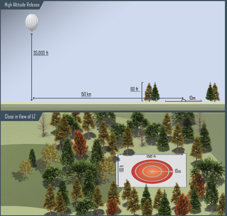 ICARUS mission. Source: DARPA-BAA-16-03
More information on ICARUS is available on the DARPA website at:
http://www.darpa.mil/program/inbound-controlled-air-reasonable-unrecoverable-systems
On 14 June 2016, Military & Aerospace reported that two ICARUS contracts had been awarded:
- PARC (Palo Alto, CA): $2.3 million Phase 1 + $1.9 million Phase 2 option
- DZYNE Technologies, Inc. (Fairfax, VA): $2.9 million Phase 1 + $3.2 million Phase 2 option
You can watch a short video describing the ICARUS competition at the following link:
https://www.youtube.com/watch?v=i2U1UTDqZbQ
The firm Otherlab (https://otherlab.com) has been involved with several DARPA projects in recent years. While I haven’t seen a DARPA announcement that Otherlab is a funded ICARUS contractor, a recent post by April Glaser on the recode website indicates that the Otherlab has developed a one-way, cardboard glider capable of delivering a small cargo to a precise target.
“When transporting vaccines or other medical supplies, the more you can pack onto the drone, the more relief you can supply,” said Star Simpson, an aeronautics research engineer at Otherlab, the group that’s building the new paper drone. If you don’t haul batteries for a return trip, you can pack more onto the drone, says Simpson.
The autonomous disposable paper drone flies like a glider, meaning it has no motor on board. It does have a small computer, as well as sensors that are programed to adjust the aircraft’s control surfaces, like on its wings or rudder, that determine where the aircraft will travel and land.”
 Sky machines. Source: Otherworld
Read the complete post on the Otherlab glider on the recode website at the following link:
http://www.recode.net/2017/1/12/14245816/disposable-drones-paper-darpa-save-your-life-otherlab
The future
The general utility of vanishing electronics, power sources and delivery vehicles is clear in the context of military applications. It will be interesting to watch the future development and deployment of integrated systems using these vanishing resources.
The use of autonomous, air-releasable, one-way delivery vehicles (vanishing or not) also should have civilian applications for special situations such as emergency response in hazardous or inaccessible areas.