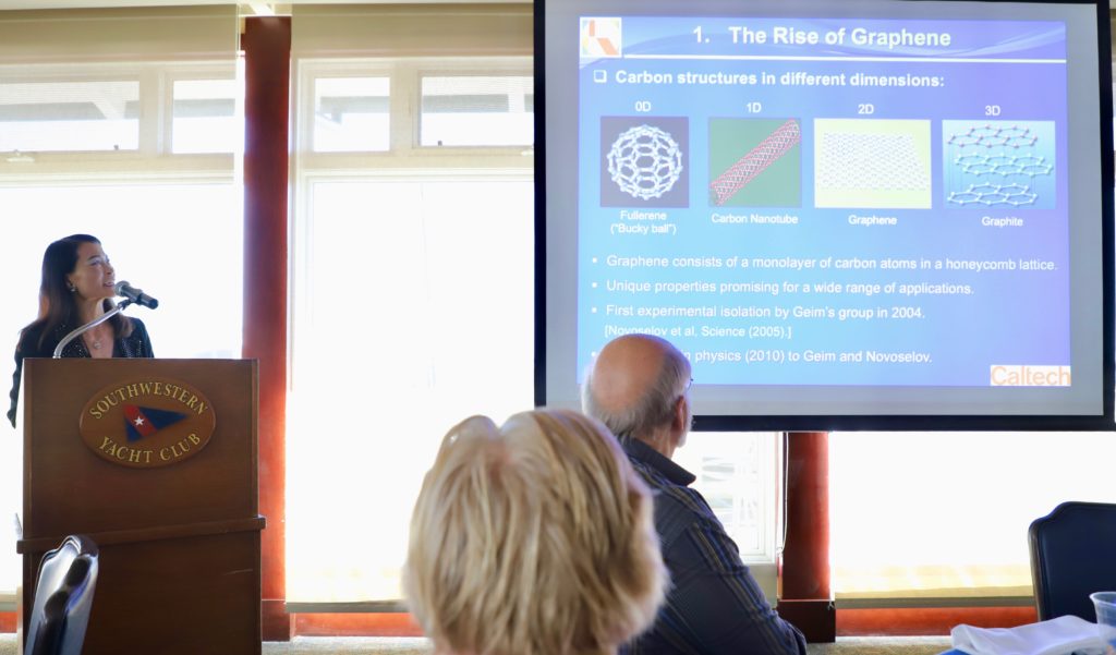
The Rise of Graphene: From Laboratory Curiosity to a Wonder Material for Science and Technology
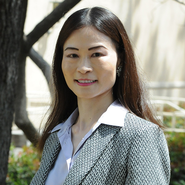
Nai-Chang Yeh
Professor of Physics
Fletcher Jones Foundation Co-Director
Kavli Nanoscience Institute
Caltech

Abstract:
Graphene, a monolayer of carbon atoms forming a two-dimensional honeycomb lattice structure, has been considered a wonder material for both scientific research and technological applications since its successful isolation in 2004. As a flexible, transparent conductor with intrinsically very high electrical mobility and thermal conductivity, graphene is promising for large-area electronic devices such as touch screen displays, electrodes for photovoltaic cells, interconnects for electrical circuits,and panels for light emitting diodes. Its unique electronic, thermal, magneticand mechanical properties and its compatibility with two-dimensional lithographic techniques are also ideal for many nano-electronic, optoelectronic,spintronic and mechanical applications. Additionally, the super-functional capability of graphene shows great potential for chemical and biological sensing, detoxification and desalination, and energy storage.

Despite all the promising aspects, one of themajor challengesto fully realize the potential of graphene-based technologies is to develop scalable and reliable methods to synthesize high-quality grapheneand graphene-based nanostructures. Much research effort worldwide has been attempted to achieve this objective, but for years it seemed that methods for reliable and high-quality production of graphene could not be used for mass production and vice versa. Since 2015, Professor Yeh’s research group at Caltech has developed breakthrough approaches to achieve scalable and single-step synthesis of 1) large-areamonolayer graphene sheets; 2) large quantity graphene nanostripes with large length-to-width aspect ratios; 3) graphene directly and selectively deposited on nanostructures; and 4) large-area bilayer graphene with controlled twisted angles. All synthesis methods are based on plasma enhanced chemical vapor deposition (PECVD) at room temperaturefor 3 ~ 15 minutes. Detailed investigations of these samples have all confirmed their excellent structural, electrical, chemical and mechanical properties.
In addition to describing the above achievements, Professor Yeh will also describe several exciting research directions in her group at Caltech that are enabled by their successful development of graphene synthesis methods, including nanoscale strain engineering of graphene for novel nano-electronics; graphene as the barrier material for next generation interconnects in ultra-large scale integration (ULSI) for the semiconducting industry; graphene nanostripes for energy storage in supercapacitors and batteries, and for energy conversion in photovoltaic cells.
Professor Yeh’s presentation can be downloaded by clicking on the link below:
Professor Yeh’s Presentation (pdf)
For more on graphene, and a link to an article in Nature about very recent work at MIT, you can click on the link below to go to the Pete’s Lynx post on 5/12/15 about graphene:
The slideshow at the beginning of the meeting, which consisted of pictures taken by Pete Lobner of the ships from the San Diego Maritime Museum sailing in San Diego harbor can be downloaded by clicking on the link below:
SD Maritime Museum Ships in SD Harbor 2018 – Lobner
Bill Hagan’s meeting slides can be downloaded by clicking on the following link:

